
SMIC工艺列表,列表中没有的工艺请电话咨询!
0.35μm logic, mixed signal/RF, high-voltage, BCD, EEPROM ,eFlash
+Technology Overview
SMIC 0.35μm process technology family includes logic, mixed signal/RF, high-voltage, BCD, EEPROM and OTP technologies. These are supported by an extensive range of libraries and IP.
Application Usage
SMIC provides cost-effective and proven solutions at the 0.35μm node for smart cards and consumer electronics and various other applications.

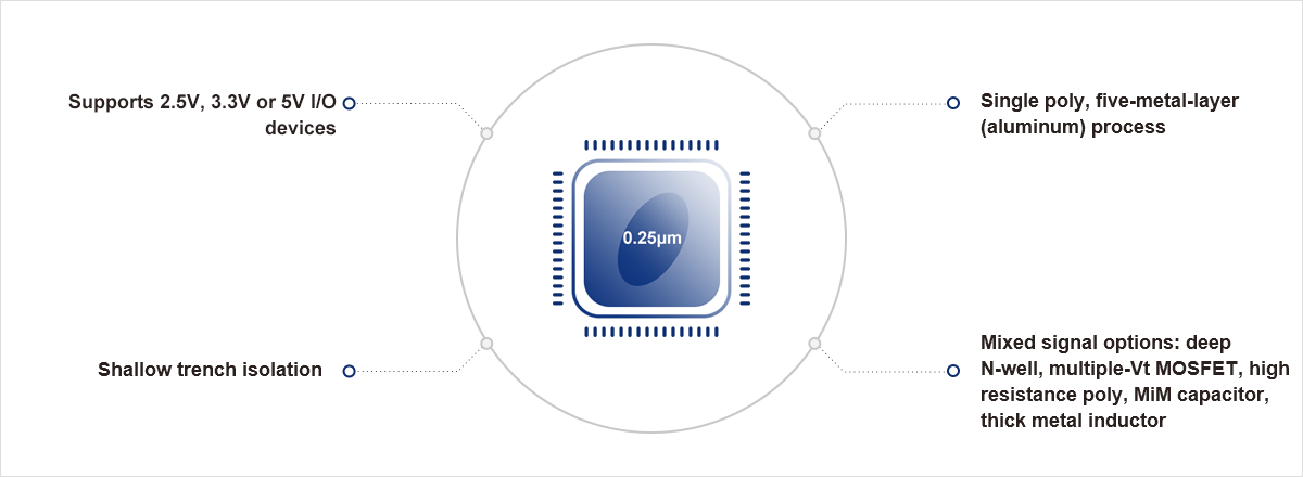
0.25μm Logic,mixed signal/RF CMOS (for 3.3V and 5V applications)
+Technology Overview
SMIC's 0.25μm technology enables high-performance, low-power integrated circuits (ICs) for high-performance graphics, microprocessors, communications, and computer data processing applications. Logic as well as mixed signal/RF CMOS (for 3.3V and 5V applications) are offered.
Features
Application Usage
SMIC provides cost-effective and proven solutions at the 0.35μm node for smart cards and consumer electronics and various other applications.

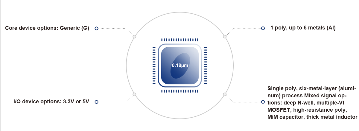
0.18μm logic, mixed signal/RF, high-voltage, BCD, EEPROM ,eFlash
+Technology Overview
Optimized for speed, power, density and cost, SMIC's 0.18μm process technology has been proven for a broad range of consumer, communications and computing applications. It also offers customers flexible solutions with modules for embedded memory, mixed signal or RF CMOS.
Using a single poly, up to six-metal-layers process, this technology features multiple voltages of 1.8V, 3.3V and 5V, and a high gate density of over 100,000 gates per mm2. Our 0.18μm process technology family includes logic, mixed signal/RF, high-voltage, BCD, EEPROM and OTP technologies. These are supported by an extensive range of libraries and IP.
Features
Application Usage
SMIC provides cost-effective and proven solutions at the 0.18μm node for smart cards, consumer electronics and various other applications.

0.15μm logic, mixed signal, high-voltage, BCD
+Technology Overview
Our 0.15μm process technology family includes logic, mixed signal, high-voltage, BCD. These are supported by extensive libraries and further IP.
Features

Application Usage
The technologies are targeted for cost-effective mobile/consumer applications and automotive and industrial applications.

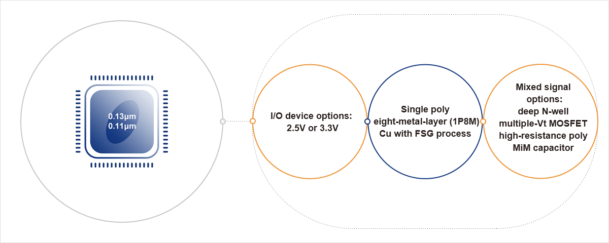
0.13/0.11μm Logic, Mixed signal, EEPROM
+Technology Overview
Compared to the same device on SMIC's 0.15μm technology, our 0.13μm technology enables a substantial die size reduction of more than 25% and performance enhancement by as much as 30%. The die size can be reduced by more than 50% and chip performance increased by more than 50% when compared to our 0.18μm technology.
SMIC's 0.13μm process technology uses an all-copper interconnect approach to drive high-performance devices while enabling cost optimization. Using eight metal layers with a poly gate length of down to 0.08μm, our 0.13μm technology offers generic devices with a core voltage of 1.2V and I/Os with supply voltage of 2.5V or 3.3V options. Low-voltage and low-leakage options are in mass production.
0.13μm/0.11µm libraries, memory compilers, I/O and analog IP are available directly from SMIC or through our network of library partners
Features
0.13μm/0.11µm Cu platform
Logic Standard Offering
0.13μm

0.11µm

Application Usage
SMIC provides cost-effective and proven solutions at the 0.13μm/0.11μm node for flash controller, media player and various other applications.

90nm Logic, Mixed signal/RF
+Technology Overview
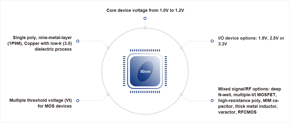
SMIC has multiple 90nm products in mass production at our 300mm facilities. With in-depth experience in process development, SMIC provides matured offerings on 90nm technology node to our customers worldwide. Our 90nm process technology uses copper interconnect, low-k material to produce high-performance devices. SMIC's 90nm production at our state-of-the-art 300mm facilities ensures cost optimization, providing our customers with additional resources for further technology enhancements. Furthermore, this technology can be customized to accommodate various design requirements including high speed, low power, mixed signal, RF, and embedded/SOI solutions.
At 90nm, SMIC provides design for manufacturing (DFM) solutions for performance enhancement and yield improvements including reliability assurance. Additionally, 90nm libraries, IP, and I/Os are all available through SMIC's network of library partners.
Features
Logic Standard Offering

Application Usage
This 90nm technology fulfills the ever-stringent requirements of power, performance, and integration for applications such as wireless handsets, digital TVs, set-top-boxes, mobile TVs, PMPs, wireless LANs and PC chipsets.

65nm/55nm logic, mixed signal, high-voltage,eFlash
+Technology Overview
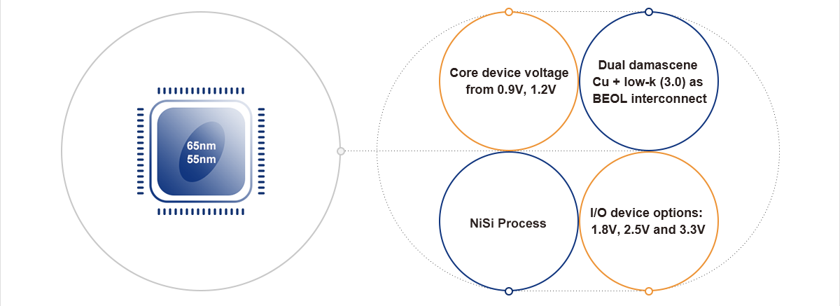
The 65nm/55nm logic technology combines improved performance and reduced power consumption with increased design possibilities and cost efficiencies. The 65nm/55nm logic process standard offerings include Low Leakage (LL) and Ultra Low Power (ULP) platforms. Both LL and ULP processes offer three threshold voltage core devices and 1.8V, 2.5V and/or 3.3V I/O options to provide a flexible design platform. Design rules, specifications, and SPICE models are available for 65nm/55nm. Critical IPs are ready for 55nm LL/ULP and 65nm LL.
Features
Logic Standard Offering

Application Usage
SMIC 55nm LL process targets a wide range of applications, such as mobile devices, computers, IoT and wearables.

40nm logic, high-voltage,eFlash
+Technology Overview
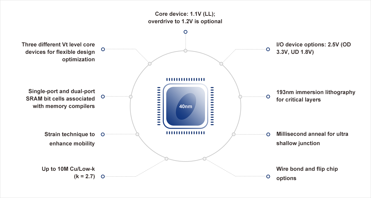
SMIC is the first foundry in mainland China to offer 40nm technology. SMIC offers its 40nm Low Leakage (LL) process with 1.1V core devices of three threshold voltage levels, as well as 2.5V I/O options (OD 3.3V, UD 1.8V), to meet various design application requirements. The 40nm logic process combines advanced immersion lithography, strain engineering technique, ultra shallow junction and low-k dielectric for power and performance optimization.
Features
Logic Standard Offering

Application Usage
SMIC 40nm LL process provides a good combination of high performance and low power solution. It diversity application scenarios covers smartphone, digital television, set-top box, game consoles and wireless connectivity applications. New additions include 40nm ULP (Ultra low power) process which is very suitable for the broader Internet of Things applications.

28nm CMOS Logic - LP,GP,HP
+echnology Overview
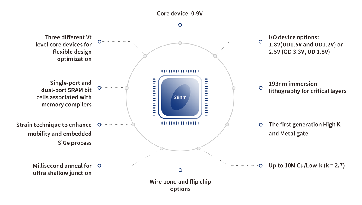
SMIC is the first Pure-Play Foundry in China to offer 28nm leading-edge advanced process technologies. SMIC's 28nm technology is a mainstream industry technology and consists of both conventional PolySiON (PS) and gate-last high-k dielectrics metal gate (HKMG) processes.
SMIC's 28nm technology had been process frozen in 4Q13 and had successfully entered the Multi Project Wafer (MPW) stage to support customer's requirements on 28nm HKMG processes. Multiple third-party IPs partners as well as SMIC's internal IPs are prepared to handle various projects from worldwide design houses.
Features
Logic Standard Offering

Application Usage
28nm process technologies primarily target mobile computing and consumer electronic related applications, such as smartphones, tablets, TVs, set-top boxes and networking. SMIC's 28nm technology supports customers on manufacturing high-performance application processors, cellular baseband, wireless connectivity, etc.


